7. Build a DA14531 or DA14585/586 Application
This section explains how the user can build, program, and run a simple software application on the ProDev Kit development board.
It provides step-by-step instructions for loading the example as a project in the Keil environment, setting it up and building it, and finally executing it via the debug environment on any of the DA14531 or DA14585/586 devices.
Make sure that you have all required tools installed as described in Section Section 5 and Section Section 6.
The DA14585/586 Software Development Kit (SDK) includes examples running on the Pro and the Basic Development Kits. The examples are provided with preconfigured KEIL projects.
The DA14531 Examples are included in the same SDK as the DA14585/586.
Note
For the DA14531 device there is a dedicated USB kit, more details in USB kit User Manual
For further reading More details are provided in the DA14531 DA14585/586 Software Developer’s Guide (UM-B-080).
Warning
To run Blinky or BLE Barebone examples you don’t need to install Dialog SmartSnippets™ Studio tool but it is a part of the full Development Environment.
7.1. The Blinky Peripheral Example Application
Blinky is a simple application which demonstrates basic initialization of DA14531 DA14585/586 and LED blinking.
After downloading the SDK, the blinky source code example can be found in the directory called peripheral_examples.
Open the folder containing the SDK files. This is the folder where you extracted the SDK zip file.
In
<sdk_root_directory>\projects\target_apps\peripheral_examples\blinky\Keil\_5, double-clickblinky.uvprojto open the project in Keil.
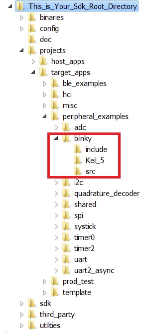
Figure 18 Blinky Project directory
The development environment should look like this when the project is opened with Keil:
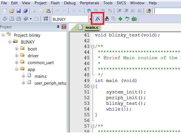
Figure 19 Blinky Project Keil Workspace
Click on the Target Options button, then click on the Device tab. The dialog should look like this.
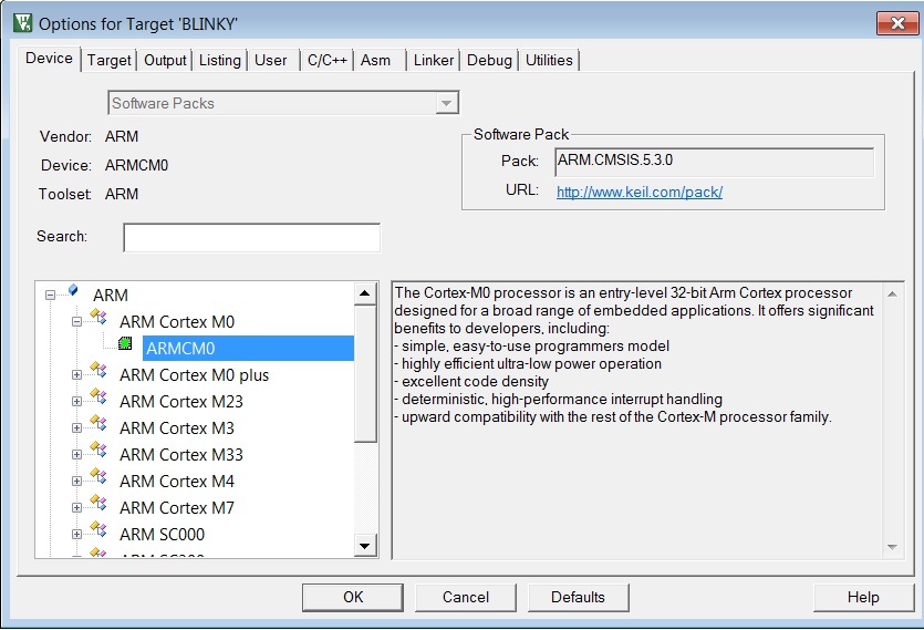
Figure 20 Blinky Project Options
Click on Linker. Scatter files (
.sct) are used for selecting memory areas.
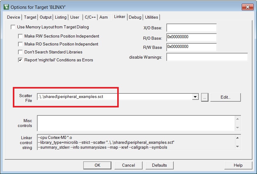
Figure 21 Blinky Project Scatter File
Click on Debug and ensure J-LINK/J-TRACE Cortex is selected and that the Initialization File is set correctly to .sysram.ini.
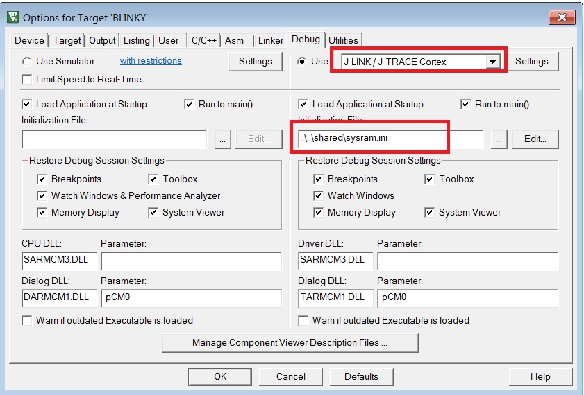
Figure 22 Blinky Project: Debug Option
Click on Settings (on the right: Debugger) and check that the SW Device has been detected correctly.
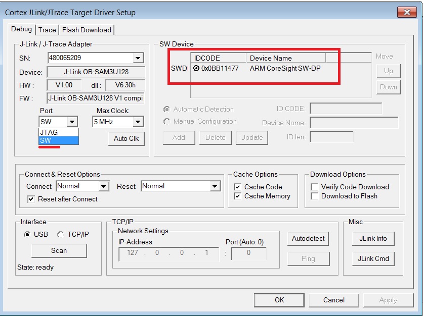
Figure 23 Blinky Project: Jlink setup
Click OK to save the settings in both windows. All settings have now been saved and you can continue to build the example.
Build the project by pressing F7 key, or clicking the Build button, see Figure 24.
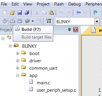
Figure 24 Blinky Project: Project Building
Make sure you have a UART connection between your PC and the motherboard, as shown in Figure 10. Check the COM number on your PC.
Open Tera Term, choose the COM port from step 9, and click OK.
In Tera Term, Select Setup > Serial Port to configure the port as shown in Table 4.
In Keil, select Debug > Start/Stop Debug Session.
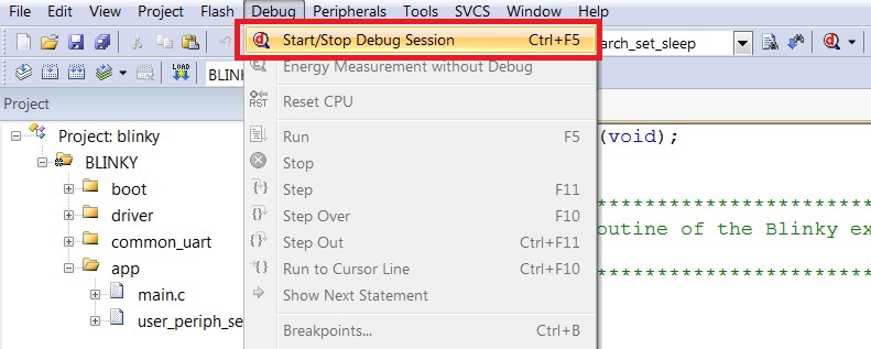
Figure 25 Blinky Project: Start Debug Session
If a non-licensed version of Keil is used, the following dialog is displayed. Click OK.
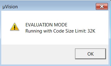
Figure 26 Keil Lite Pop Up Window
Press F5 or click the Run button to start code execution.
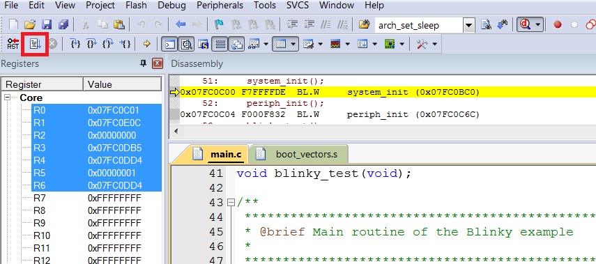
Figure 27 Blinky Project: Code Execution
When the blinky message is displayed on your UART terminal screen and the green LED is blinking you have successfully programmed and started the blinky program on DA14531 or DA14585/586 Demo board. Use the same Default Jumper configuration as shown in Figure 4.
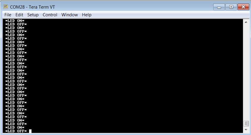
Figure 28 Blinky Project: Blinky message on COM28 terminal
Note
The whole application is placed/executed in RAM. For more details about RAM management you can refer to How to change the RAM size Tutorial.
Note
SPI Flash (U8: See Figure 6) can also be used for downloading an image file (a .hex or .bin). for SPI flash programming steps using SmartSnippets Toolbox you can refer to UM-B-080: Section 6.8: SPI Flash Memory Example and for SPI flash programming Keil example you can refer to UM-B-083: Section 13: SPI Flash Programmer. The Figure 29 shows the Jumper setting for the J5 when using SPI configuration for the DA14585/586.
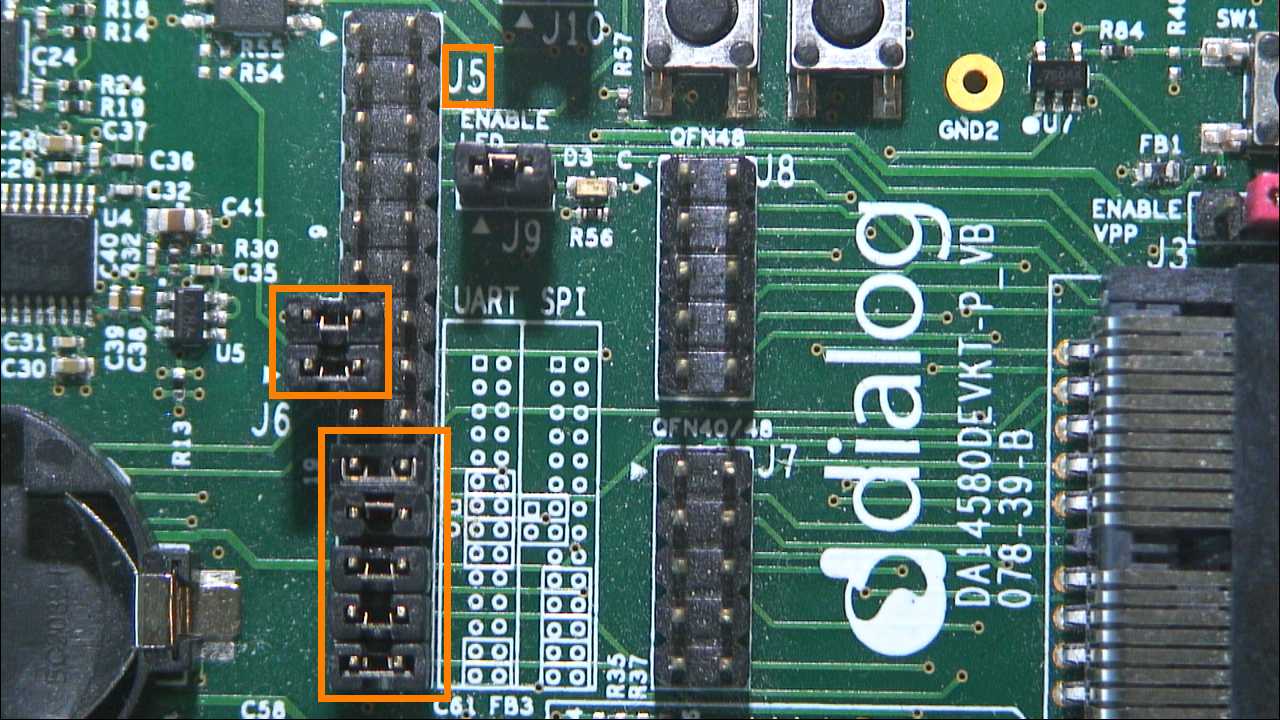
Figure 29 DA14585/586 J5 Jumper setting for SPI flash programming
Warning
For the DA14585/586 P0_5 and P0_6 ports are used for the SPI flash connection.
The DA14531 is using different SPI Flash assignment pins (different booting sequence) : P0_0 (MOSI) and P0_3 (MISO). You can refer to AN-B-072 DA14531 Booting from serial interfaces
7.2. The Barebone BLE Example Application
The Barebone BLE example application demonstrates basic BLE procedures such as advertising, connection, updating connection parameters, and implementation of the Device Information Service Server (DISS). For further reading See the Bluetooth SIG for more details.
Open the folder containing the SDK files. This is the folder where you extracted the SDK zip file.
In
<sdk_root_directory>\projects\target_apps\ble_examples\ble_app_barebone\Keil_5, double-clickble_app_barebone.uvprojto open the project in Keil.
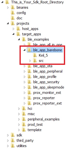
Figure 30 Barebone BLE Project directory
Figure 31 shows the Keil project layout.
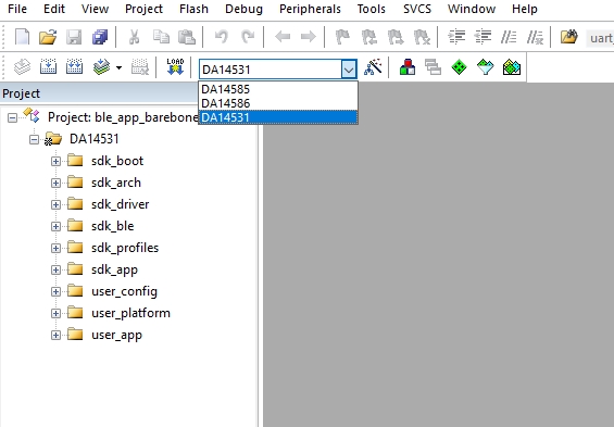
Figure 31 Barebone BLE: KEIL Project Layout
To execute the code and run the example, repeat steps 3 to 14 in The Blinky Peripheral Example Application.
The barebone application does not use the UART and so the only jumpers required are those for the debugger interface as noted in Table 6.
Use the Android application BLE Scanner to scan for, and connect to, the DIALOG-BRBN app, see Figure 32.
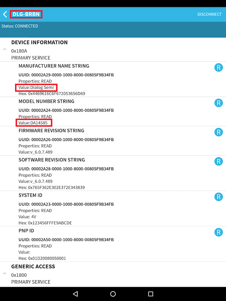
Figure 32 Barebone BLE: Interacting with BLE Application
Your BLE application is now running and advertising using the default advertiser string: “DIALOG-BRBN”.
Note
In this example, we used an Android application but you can also use the LightBlue iOS application to connect an iPad/iPod/iPhone device to the application.
Note
When you change the advertising name of your device and you don’t want your iPhone/iPad.. to connect to it anymore, it’s easy to make your device forget about it. Follow easy steps mentioned in the Apple Support Communities and your iPhone won’t remember your Bluetooth device. If you change your mind, no worries, you can pair the device as though it were new.
Warning
When multiple device use the same BD address in the same room test, it is highly recommended to changes manually your BD address or use the static random address (advanced) to avoid any conflict, You can refer to Tutorial 1: Advertising contents
7.3. Troubleshooting
If you can’t see any blinky messages in your UART terminal and the LED is not blinking, check the UART and LED jumper configuration, see Table 5.
GPIO |
Function |
Jumper |
|---|---|---|
P0_4 |
UART2 TX |
Connect J5.11 - J5.12 |
P0_5 |
UART2 RX |
Connect J5.13 - J5.14 |
P1_0 |
LED |
Connect J9.1 – J9.2 |
If you can’t start a debug session, check the SWD debugger jumper configuration, see Table 6.
JTAG |
Function |
Jumper |
|---|---|---|
TMS |
SWD IO |
Connect J5.25 - J5.26 |
TCK |
SWD CLK |
Connect J5.27 - J5.28 |
If you have trouble with the J-link firmware or any issue with SDK operation, refer to the DA1458x/68x Development Kit J-Link Interface Application Note AN-B-052.
Note
If none of these actions resolved the issue, please contact Dialog Software Forum.
7.4. What Next ?
This tutorial does not cover all the topics relevant to software development environments, it describes the first steps necessary to get started with the Pro Development Kit. The following links provide more information on DA14585/586:
DA14585 Product Brief: To know more about the SmartBond™ DA14585 SoC.
DA14586 Product Brief: To know more about the SmartBond™ DA14586 SoC.
DA14531 Product Brief: To know more about the SmartBond™ DA14531 SoC.
UM-B-079: DA14531 DA14585/586 SDK 6 Software Platform Reference: To know more about software architecture.
UM-B-080: DA14531 DA14585/586 SDK 6 Software Developer’s Guide: To build more BLE and peripheral examples.
Codeless Tutorial: To quick start your IoT application and learn more about AT commands.
DA14585/586 Sleep mode configurations and power measurement: To learn more DA14585/586 Power management.
DA14585/586 Application Hardware Design Guideline : To learn how to prepare schematics and PCB layouts for your application.
DA14585/586 Interfacing with external memory : To learn s how to use an external memory (I2C EEPROM or SPI Flash) with the DA14585/586.
DA14531 Sleep mode configurations and power measurement: To learn more DA14531 Power management.
DA14531 Application Hardware Design Guideline : To learn how to prepare schematics and PCB layouts for your application.
Interfacing with external memory : To learn s how to use an external memory (I2C EEPROM or SPI Flash) with the DA14531.