4. The DA14531 and DA14585/586 Hardware
The DA14585/586 Pro Development Kit DA14585/586 ProDev Kit consists of a motherboard (MB-PRO) and a DA14585 daughterboard featuring the DA14585/586 SoC of the desired package, WLCSP34 or QFN40.
The DA14531 Pro Development Kit DA14531 ProDev Kit consists of a the same motherboard (MB-PRO) and a DA14531 daughterboard featuring the DA14531 SoC of the desired package, WLCSP17 or QFN24.
4.1. The ProDev Kit Motherboard
Figure 1 illustrates the physical layout of the ProDev Kit motherboard Rev C. The Figure 6 shows The DA14585/586 ProDK combined with the the DA14585 daughterboard.
and the Figure 7 shows The DA14531 ProDK combined with the the DA14531 daughterboard.
The ProDev Kit Motherboard provides the necessary hardware to enable:
full digital connectivity with external hardware using UART, SPI, GPIO, and I2C
USB based debugging capabilities using the SEGGER J-Link on-board debugger
USB based UART communication with the host PC using a Future Technology Devices International (FTDI) chipset which converts UART to USB signal.
Note
The DA14531, DA14580 and the DA14585/586 share the same ProDev Kit motherboard (DA14580 DEVKT).
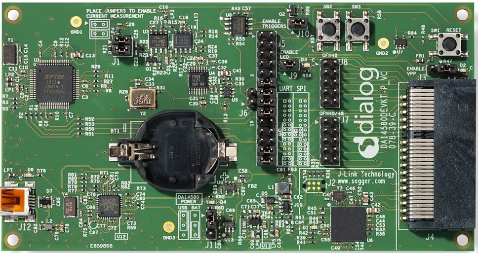
Figure 1 The DA14585/586 ProDev Kit Motherboard
4.2. The DA14585/586 Pro Kit daughterboard
Figure 2 presents the DA14585/586 Daughterboard.

Figure 2 DA14585/586 Daughterboard
Reference |
Description |
|---|---|
1 |
Bluetooth Antenna |
2 |
U1: BLE Processor DA14585 |
3 |
Y1: 16MHz |
4 |
Y2: 32.768 KHz |
5 |
PCI-e |
4.3. The DA14531 Pro Kit daughterboard
Figure 3 presents the DA14531 Daughterboard.

Figure 3 The DA14531 Daughterboard
Reference |
Description |
|---|---|
1 |
|
2 |
|
3 |
|
4 |
|
5 |
Note
The AN-B-073 contains guidelines for implementing a RFIO filter to reduce conducted and radiated spurious emissions in Bluetooth low energy applications.
4.4. Configuring the Pro Kit Board by Jumper Settings
The DA14585/586 supports booting from UART. The jumper settings are displayed below:

Figure 4 DA14585/586 Jumper Setting
Figure 5 shows the layout of the header jumper, J5.

Figure 5 Jumper J5 Layout
Jumper |
Default Position |
Comment |
|---|---|---|
J1 |
Placed |
Enable Current Measurement |
J3 |
Not Placed |
VPP Enable |
J5.11 – J5.12 |
Placed |
TxD (P0_4) |
J5.13 – J5.14 |
Placed |
RxD (P0_5) |
J5.15 – J5.16 |
Placed |
CTS (P0_6) |
J5.17 – J5.18 |
Placed |
RTS (P0_7) |
J5.25 – J5.26 |
Placed |
T_TMS (SWDIO) |
J5.27 – J5.28 |
Placed |
T_TCK (SWCLK) |
J7 |
Not Placed |
QFN40/48 |
J8 |
Not Placed |
QFN48 |
J9 |
Placed |
LED Enable |
J10 |
Placed |
Enable Triggers |
J11 |
Placed |
BATT/USB |
4.5. Board Layout
The layout of the boards is displayed in Figure 6.

Figure 6 DA14585/586 Board Layout
Figure 7 DA14531 Board Layout
Note
The schematic diagrams, BOM, and Gerber files are illustrated in detail in the Development Kit Documentation.
4.6. Connecting the ProDev Kit to the host PC
The ProDev Kit motherboard includes FTDI chipset U1 FT2232HL which allow easy communication with the development host over USB. The FT2232HL implements the USB to UART function and ensure the connectivity of PC to the DA14585/586 SoC UART port and to current sense circuitry through SPI connection with ADC U4.
The chip is supplied with a 3.3V from U13. A 12MHz crystal Y1 is required for the chip operation.
The ProDev Kit motherboard also includes an embedded J-Link debugger U6 SAM3U2CA. The chip is supplied with a 3.3V from U13 which is enabled by PWR_ENABLE signal.
Before connecting the ProDev Kit to the host PC, make sure that the motherboard and the desired daughterboard module are properly connected.
A choice can be made between 3.3 V (via USB: J11 1-2) or VDD (a coin cell: J11 2-3). No battery is needed when running via the mini-USB cable.
The ProDK Development Kit is connected to the host PC over the connector marked as USB1, as shown in reference 6 in Figure 8 using a standard mini-USB

Figure 8 ProDK Development Kit connections
Note
The ProDev Kit is connected to the host PC over the connector marked as USB (J12), as shown in Figure 6 using a standard mini-USB cable.
When mounting a battery on the daughterboard, Jumper J11 should be fitted on 2-3 position.
For proper battery functionality, a small modification should be made. See the workaround in Appendix C.